| 2.6. Micro Abilis C3 | ||
|---|---|---|
 | Chapter 2. Abilis hardware |  |
| 2.6. Micro Abilis C3 | ||
|---|---|---|
| | Chapter 2. Abilis hardware | |
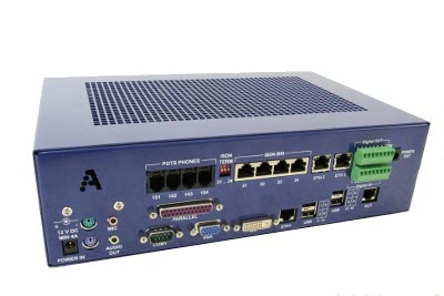
Micro Abilis is a non-expandable device equipped with:
1 ELTI;
4 USB ports;
4 BRI;
4 POTS.
Table 2.1.
| Led | Meaning | State |
|---|---|---|
LIVE AUX | Abilis Status Not used | LIVE and AUX leds flashing: startup LIVE led flashing (1s ON - 1s OFF): Abilis status is ok AUX led: not used |
![[Warning]](../images/warning.png) | Warning |
|---|---|
|
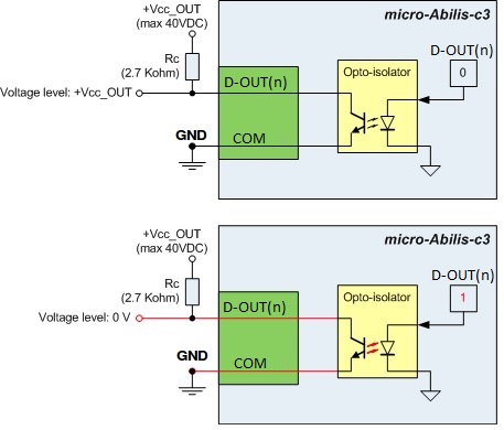
Each one of the D-OUT[7..1] is an
opto-isolated driver:
when activated (D-OUT[n]=1), it
internally connects the corresponding pin to the
"COM" pin
when deactivated (D-OUT[n]=0), its
voltage level is floating, like an open circuit
It is necessary to implement an active circuit before connecting
the D-OUTn to any actuator, i.e. an externally
powered circuit that uses amplifiers and relays to drive lamps,
motors, gate locks or other electric devices. The picture below shows
the internal implementation of the D-OUT driver.
+Vcc_OUT must be lower than 40VDC (in order not to damage the internal
opto-isolator), while the current flowing from
D-OUTn to COM must never be
greater than 15 mA. Resistor Rc must be calculated in order to provide
a max current of 15mA when the max voltage is applied. For example an
Rc value of 2.7 KOhm is suitable for most applications.
| Warning |
|---|---|
DO NOT INVERT THE POLARITY: voltage on
|
![[Tip]](../images/tip.png) | Tip |
|---|---|
Interesting chapter: Section 14.1.3, “Activating MFIO resource”. |
| Warning |
|---|---|
Pay attention to the circuit recommendations in the following sections |
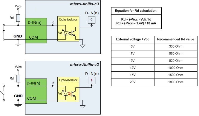
Digital Inputs are opto-isolated too. They too must be driven using an externally-powered circuit as well as Digital Outputs.
Depending on how much current the circuit drives into the
D-IN pin, the corresponding
D-INn bit will return:
0 when less than 10 uA flows from D-INn
to COM
1 when more than 1 mA flows from D-INn to
COM
The picture below shows the internal implementation of the
D-IN. Resistor Rd must be chosen considering the
+Vcc voltage applied. The picture below shows the suggested Rd values
at different +Vcc voltages. The current flowing from
D-INn to COM must never be
greater than 20 mA.
| Warning |
|---|---|
The maximum driving current supported by the photo diode is 20mA! |
| Tip |
|---|---|
Interesting chapter: Section 14.1.3, “Activating MFIO resource”. |
| |  | |
| 2.5. Pico Abilis |  | 2.7. MFIDE module |